Hardware Specification
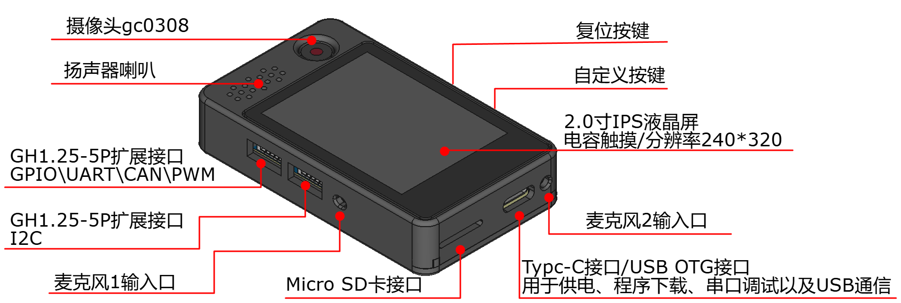
Development Board Overview
-
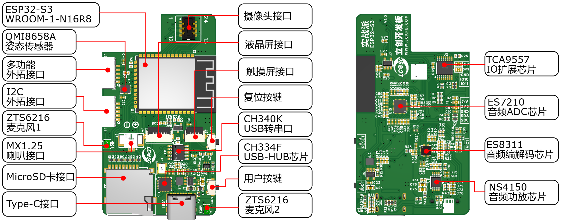
Main Control Chip
- The development board is powered by the ESP32-S3, utilizing the Espressif ESP32-S3-WROOM-1-N16R8 module, which includes 16MB of FLASH and 8MB of PSRAM.
-
Camera
- Integrated GC0308 camera with 300,000 pixels.
-
Display:
- LCD Screen: 2.0-inch IPS high-definition color display, suitable for various display applications.
- Touch Screen: Capacitive touch screen enabling finger control applications.
-
Audio:
- Integrated audio chips ES7210 and ES8311.
- Dual microphone inputs with hardware echo cancellation.
- 1W speaker for audio playback.
-
Sensors
- Integrated 6D attitude sensor QMI8658 for detecting the board's orientation.
-
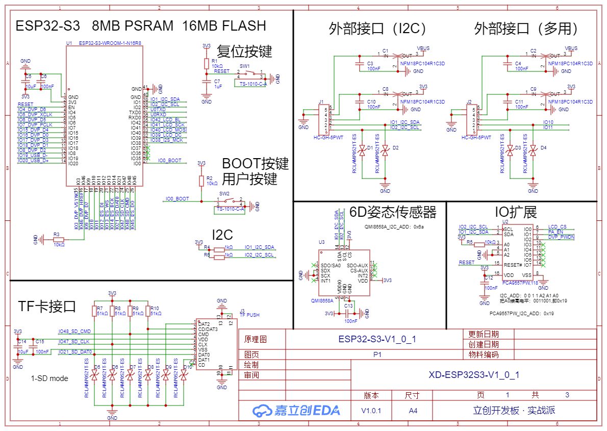
Expansion Interfaces:
- I2C Interface: Connects to external sensors supporting I2C communication.
- Multi-function Interface: Exposes two ESP32 GPIO pins, configurable as general GPIOs, UART, I2C, CAN, PWM, etc.
-
TF Card Interface: Supports 1-SD mode connection.
-
USB-HUB Chip: Integrates ESP32's serial and USB ports via a TYPE-C interface, facilitating power supply, programming, data observation, and USB device communication with a single cable.
-
Dual Power Supply: Separate power supplies for MCU and audio circuits.
-
Buttons: One reset button and one user-defined button.
-
AI Capabilities: ESP32-S3 supports AI functions like voice and image recognition. Combined with Wi-Fi and Bluetooth features, the board enables various interesting applications.
Schematic
Box 3D file
Schematic Introduction
MCU GPIO Names
The development board uses the ESP32-S3-WROOM-1-N16R8 module. The diagram below shows the module's schematic. The module has already integrated the ESP32-S3 chip, FLASH chip, as well as peripheral circuits and antennas, so the diagram is quite simple here.
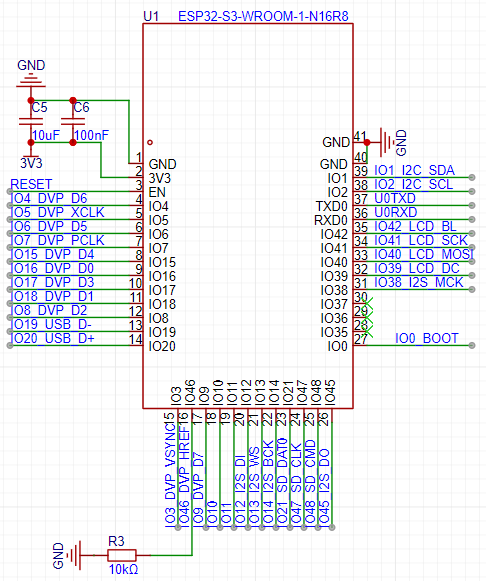
The pin network label names adopt the format of GPIO number + peripheral function. This naming method is beneficial because you can know the purpose of the pin and its GPIO number just by looking at the name, making it very friendly for programming.
For the IO46 pin, in download mode, it must be at a low level; otherwise, the program cannot be downloaded. Here, a pull-down resistor is connected to the IO46 pin to ensure it remains at a low level when the pin state is not controlled. When designing circuits, you should also note that if IO46 is connected to another chip, the pin connected to IO46 should either be high-impedance by default after power-on or remain at a low level.
The module uses an 8-bit PSRAM chip. The IO35, 36, and 37 pins are already used by the PSRAM pins, so they cannot be used here and will remain unused.
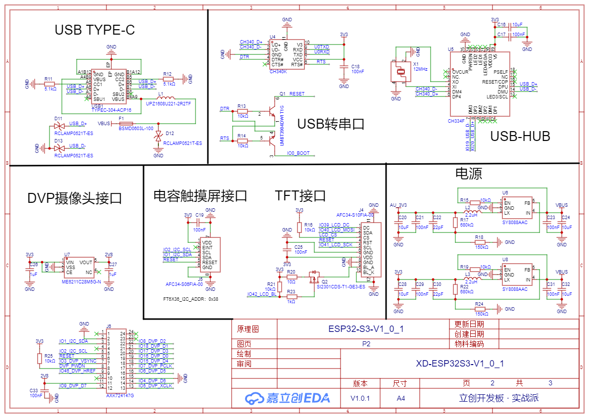
USB Subsystem
The diagram below shows the USB-HUB circuit.
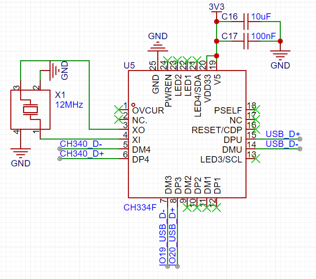
The CH334F is a 4-port USB hub chip with 4 USB2.0 downstream interfaces. Here, we only use 2 downstream interfaces. The TYPE-C port on the development board is connected to the chip's upstream interface, which is USB_D+ and USB_D- in the figure. Downstream interface D4 is connected to the USB-to-serial chip, and downstream interface D3 is connected to the ESP32's USB-OTG interface.
The hub chip does not require a driver and can be automatically recognized on WIN10 and Linux systems.
The diagram below shows the USB-to-serial circuit, connected to ESP32's serial port 0, which can achieve automatic program downloading and serial terminal debugging functions. The USB-to-serial chip uses CH340K, which requires a driver to be installed for use.
CH340K driver download address: https://www.wch.cn/downloads/CH341SER_EXE.html
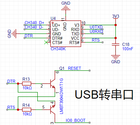
If connect the device to a PC, there will be two COM ports:
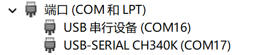
One is the USB-UART bridge, the other is the USB-OTG interface.
Input/Output Interfaces
The diagram below shows the button circuit, with a total of two buttons: a reset button and a user button.
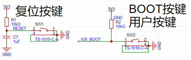
The reset button restarts the microcontroller. The user button can be used to implement custom functions. Without the previous automatic program download circuit, when downloading a program, you need to press the BOOT button without releasing it, then press RESET to start downloading. Since BOOT and RESET are already controlled by the automatic download circuit, the BOOT button here is actually a user button and can be used for custom input functions.
Display & Touch
The diagram below shows the LCD and touch screen interface circuit.
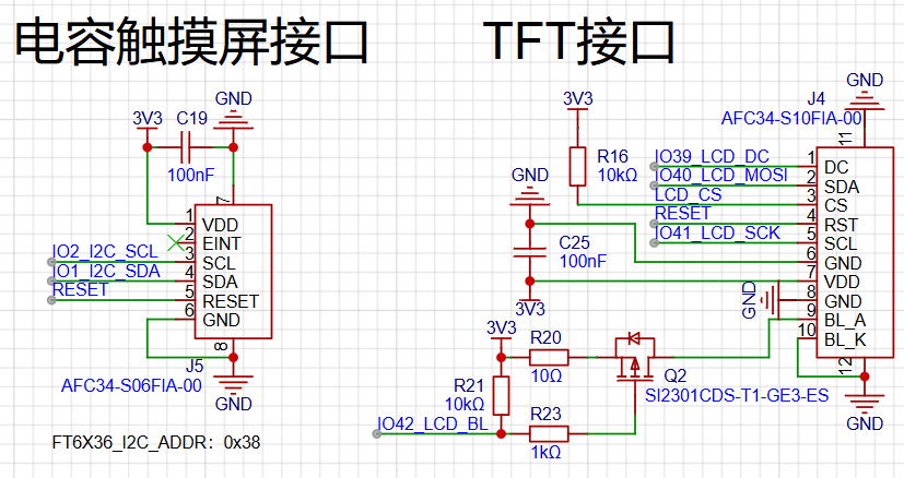
The LCD uses SPI communication, and the touch screen uses I2C communication. The LCD supports program control for turning the backlight on and off and PWM brightness adjustment.
Camera Interface (GC0308)
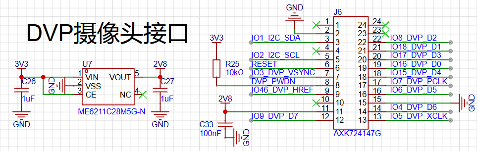
The diagram below shows the camera interface, using a BTB connector. The camera uses the GC0308. The GC0308 only requires a single power supply of 2.8V.
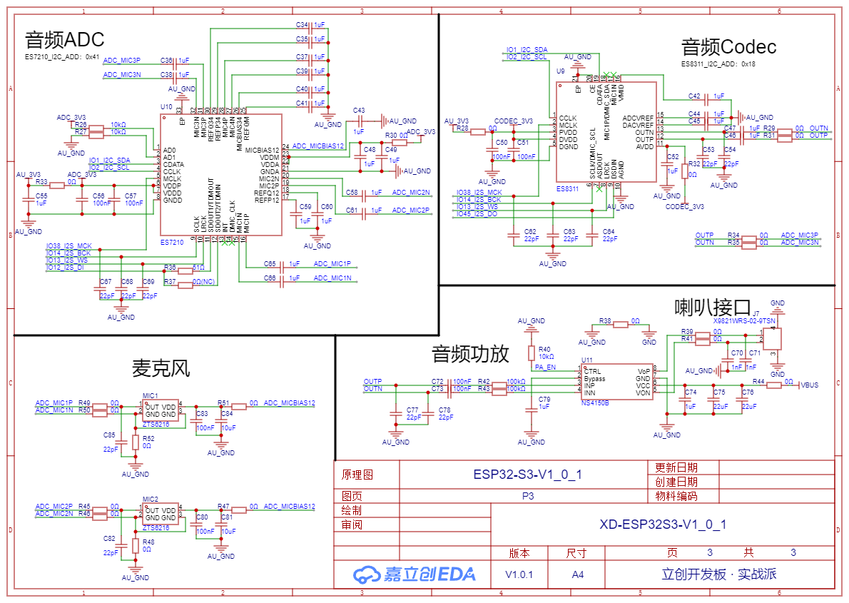
Audio Pipeline
The audio circuit is divided into ADC input (MIC) and DAC output (speaker).
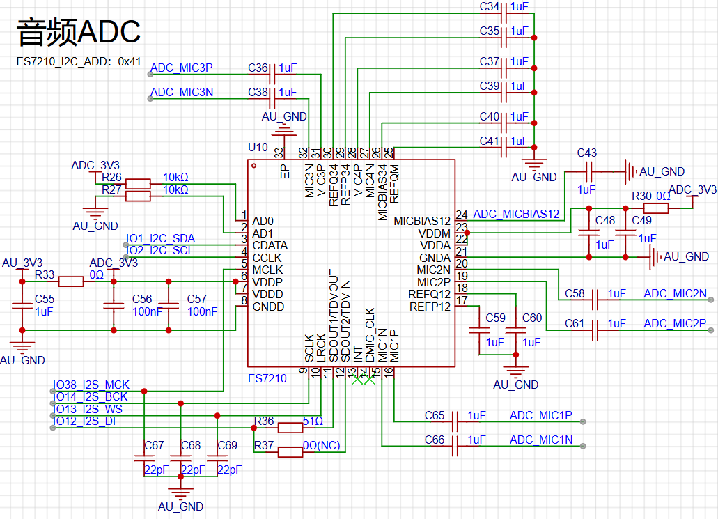
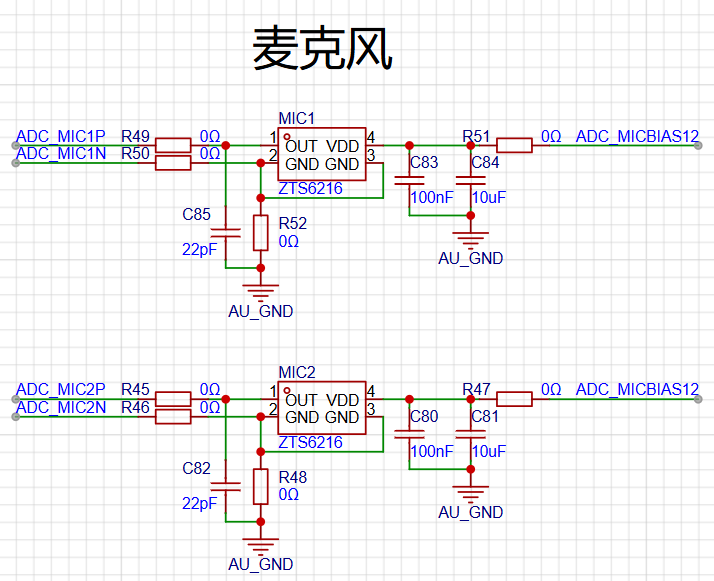
The diagram below shows the audio ADC circuit, with the audio chip model being ES7210. It supports 4 MIC inputs, and here we use 3 of them. Two are connected to MICs, and one is connected to DAC output for echo cancellation.
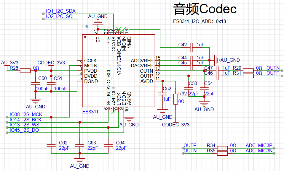
The diagram below shows the audio DAC circuit, with the chip model being ES8310. ES8310 supports both ADC and DAC. Here, we do not use its MIC input but only its audio output function. Its output goes to two places: one to the MIC3 input of ES7210, and the other to the audio amplifier output.
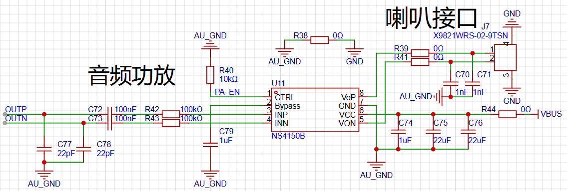
The diagram below shows the audio amplifier output circuit, with the chip model being NS4150B. The PA_EN pin is pulled low by default, turning off the speaker output.
Power Management
The diagram below shows the dual power supply circuit.
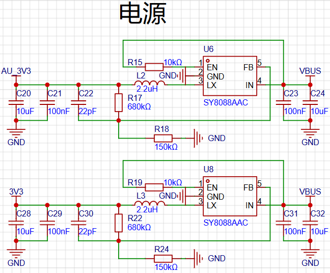
The audio circuit uses AU_3V3 power, while other circuits use 3V3 power.
Attitude Sensor
The diagram below shows the attitude sensor circuit.
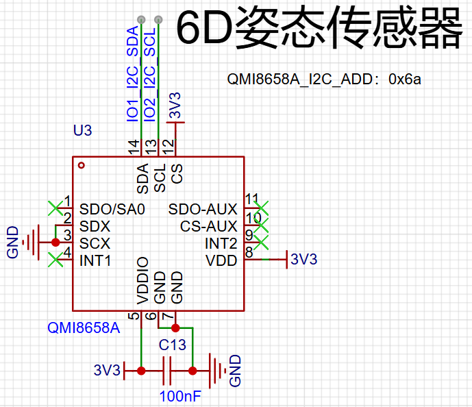
The development board, when combined with an attitude sensor, can be used for many intelligent projects, such as detecting when the board is picked up by hand, whether it is upright or lying flat, or whether it is stationary or in motion, etc.
IO expansion Chip
The diagram below shows the IO expansion chip circuit.
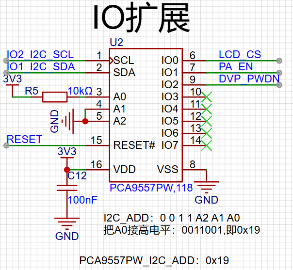
This expansion chip has an I2C interface and can expand 8 IO ports. Here, we only use 3. LCD_CS controls the LCD, PA_EN controls the audio amplifier switch, and DVP_PWDN controls the camera switch. Therefore, if your application requires the use of the LCD, audio output, or camera, you must first activate the IO expansion driver.
TF card interface
The diagram below shows the TF card interface circuit.
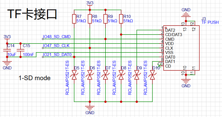
The TF card uses 1-SD mode to communicate with the ESP32, requiring only the CMD, CLK, and DAT0 pins. Although other data pins are not used for communication, ESD chips are still needed to prevent damage to the TF card during insertion and removal. Additionally, the DAT3 pin should be connected to a pull-up resistor because when DAT3 is high, the TF card operates in SD mode, and when DAT3 is low, the TF card operates in SPI mode. Here, we need the TF card to work in SD mode.
External expansion interface
The diagram below shows the external expansion interface circuit.
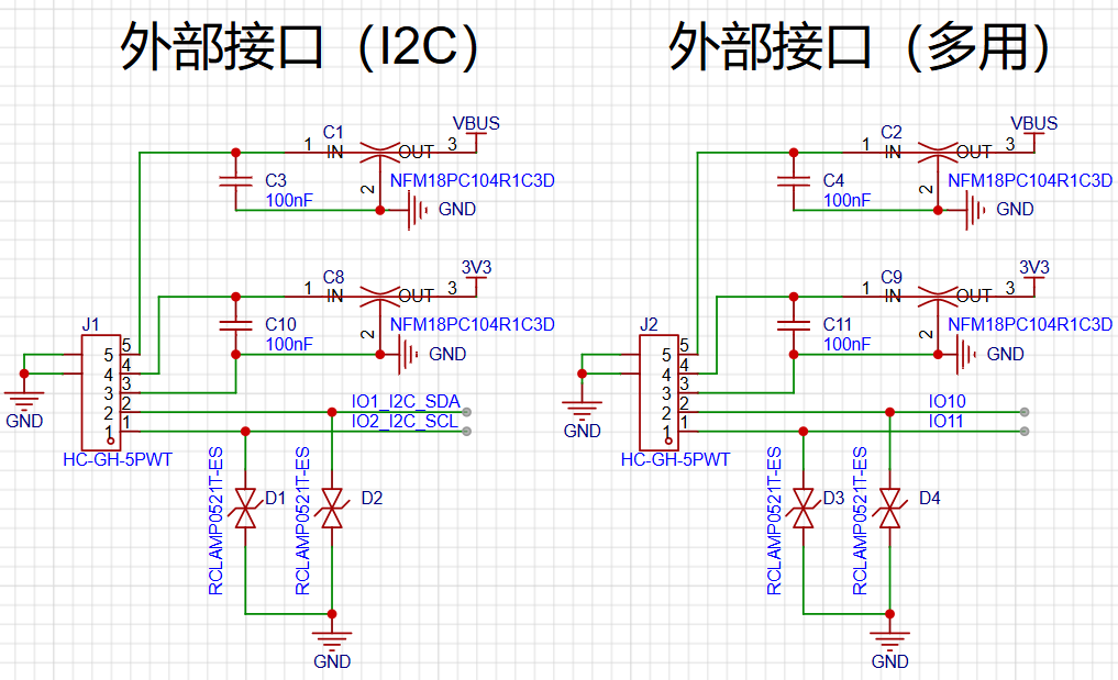
The development board has two expansion interfaces: one is an I2C interface, and the other is a multifunction custom interface. They use 5P GH terminals, capable of providing 3.3V and 5V for powering external sensors.
The I2C interface shares the same I2C interface as the attitude sensor, capacitive touch screen, and audio chip, so it can only be used as an I2C interface and should not be repurposed for other functions.
The other multifunction interface outputs GPIO10 and 11, which can be used as general GPIOs or repurposed as serial ports, I2C ports, CAN ports, PWM ports, etc.